ISL6112
18
FN6456.1
August 25, 2011
Fault Reporting and Interrupt Generation
SMI-ONLY CONTROL APPLICATIONS
For applications in which the ISL6112 is controlled only by SMI,
ON and AUXEN are connected to GND, and the FORCE_ON
pins
are either shorted or are connected to V
STBY
as shown in
Figure27. In these cases, the ISL6112 FAULT
outputs and
STATUS Register Bit D[7] (FAULT) are not activated, because fault
status is determined by polling STATUS Register Bits D[4], D[2],
D[0] and CS (Common Status) Register Bits D[2:1]. Individual
fault bits in the STATUS and CS registers are asserted after POR,
when:
"Either or both CNTRL Register Bits D[1:0] are asserted, AND
"12VIN, 3VIN, or VSTBY input voltage is lower than its respective
ULVO threshold, OR
"The fast OC circuit isolation protection has tripped, OR
"The slow OC circuit isolation protection has tripped AND its
filter time-out has expired, OR
"The slow OC circuit isolation protection has tripped AND Slot
die temperature > +140癈, OR
"The ISL6112 global die temperature > +160癈
Once asserted, to clear any one or all STATUS Register Bits D[4],
D[2], D[0] or CS Register Bits D[2], D[1], a software subroutine
can perform an
echo reset
in which a Logical
1
is written
back to those register bit locations that have indicated a fault.
This method of
echo reset
allows data to be retained in the
STATUS and/or CS registers until such time as the system is
prepared to operate on that data.
The ISL6112 can operate in interrupt mode or polled mode. For
interrupt-mode operation, the open-drain, active-LOW INT
output
signal is activated after POR if the INTMSK bit (CS Register Bit
D[3]) has been reset to Logical
0
. Once activated, the INT
output is asserted by any one of the fault conditions previously
listed. It is deasserted when one or all STATUS Register Bits D[4],
D[2], D[0] or CS Register Bits D[2], D[1] are reset upon the
execution of an SMBus
echo reset
WRITE_BYTE cycle. For
polled-mode operation, the INTMSK bit should be set to Logical
1,
thereby inhibiting INT
output pin operation.
For SMI control applications in which the FORCE_ON
inputs are
needed for diagnostic purposes, the FORCE_ON
inputs must be
enabled; that is, CNTRL Register Bit D[2] should read Logical
0.
Once FORCE_ON
inputs are asserted, all output voltages are
present with all circuit protection features disabled, including
over-temperature protection on VAUX outputs. To inhibit
FORCE_ON
operation, a Logical
1
is written to the CNTRL
Register Bit D[2] locations.
HPI-ONLY CONTROL APPLICATIONS
For applications in which the ISL6112 is controlled only by HPI,
SMBus signals SCL, SDA, and INT
are connected to V
STBY
as
shown in Figure 27. In this configuration, the ISL6112 FAULT
outputs are activated after POR and become asserted when:
Either or both external ON and AUXEN input signals are asserted,
AND
"12VIN, 3VIN, or VSTBY input voltage is lower than its respective
ULVO threshold, OR
"The fast OC circuit isolation protection has tripped, OR
"The slow OC circuit isolation protection has tripped AND its
filter time-out has expired, OR
"The slow OC circuit isolation protection has tripped AND slot
die temperature > +140癈, OR
"The ISL6112 global die temperature > +160癈.
To clear FAULT
outputs, once asserted, either or both ON and
AUXEN input signals must be deasserted. (See FAULT
pin in
Pin
Descriptions
table on page4 for additional information.) If the
FORCE_ON
inputs are used for diagnostic purposes, both the
FAULT
and PWRGD
outputs are deasserted after the FORCE_ON
inputs are asserted.
Serial Port Operation
The ISL6112 uses standard SMBus Write_Byte and Read_Byte
operations for communication with its host. The SMBus
Write_Byte operation involves sending the devices target
address, with the R/W
bit (LSB) set to the low (write) state,
followed by a command byte and a data byte. The SMBus
Read_Byte operation is similar, but it is a composite write and
read operation. The host first sends the devices target address,
followed by the command byte, as in a write operation. A new
VSTBY
PWRGD
AUXEN
(1)
ON
(1)
FORCE_ON
(1)
(1) EXTERNAL PIN
(2) CNTRL REGISTER BIT D[0]
(3) INTERNAL FLAG
(4) CNTRL REGISTER BIT D[1]
(5) CNTRL REGISTER BIT D[2]
MAIN
(4)
VAUX
(2)
3VAUX_UV
(3)
FORCE_EN
(5)
12VOUT_UV
(3)
3VOUT_UV
(3)
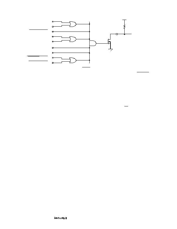
FIGURE 30. PWRGD
LOGIC DIAGRAM
发布紧急采购,3分钟左右您将得到回复。
相关PDF资料
ISL6114IRZA
IC HOT PLUG CTRLR PCI-E 48-QFN
4006-020
LED CONST CURRENT RESISTOR 20MA
A8450KLBTR-T
IC REG QD BUCK/LINEAR 24-SOIC
AD595CD
IC THERMOCOUPLE INSTR AMP 14CDIP
AD597AHZ
IC THERMOCOUPLE COND TO-100-10
AD7314ARMZ-REEL7
IC SENSOR TEMP 10BIT DGTL 8-MSOP
AD7814ARTZ-REEL
IC TEMP SNSR 10BIT DGTL SOT23-6
AD7818ARZ
IC ADC 10BIT W/TEMP SENSOR 8SOIC
相关代理商/技术参数
ISL6112IRZA
功能描述:热插拔功率分布 8LD 7X7 DL SLOT PCI EXPR HOT PLUG CONTRO RoHS:否 制造商:Texas Instruments 产品:Controllers & Switches 电流限制: 电源电压-最大:7 V 电源电压-最小:- 0.3 V 工作温度范围: 功率耗散: 安装风格:SMD/SMT 封装 / 箱体:MSOP-8 封装:Tube
ISL6112IRZA-T
功能描述:热插拔功率分布 8LD 7X7 DL SLOT PCI EXPR HOT PLUG CONTRO RoHS:否 制造商:Texas Instruments 产品:Controllers & Switches 电流限制: 电源电压-最大:7 V 电源电压-最小:- 0.3 V 工作温度范围: 功率耗散: 安装风格:SMD/SMT 封装 / 箱体:MSOP-8 封装:Tube
ISL6113
制造商:INTERSIL 制造商全称:Intersil Corporation 功能描述:Dual Slot PCI-E Hot Plug Controllers
ISL6113EVAL1Z
制造商:INTERSIL 制造商全称:Intersil Corporation 功能描述:Dual Slot PCI-E Hot Plug Controllers
ISL6113IRZA
功能描述:热插拔功率分布 4 8LD 7X7 DL SLOT PCI-E HOT PLUG CNTRL RoHS:否 制造商:Texas Instruments 产品:Controllers & Switches 电流限制: 电源电压-最大:7 V 电源电压-最小:- 0.3 V 工作温度范围: 功率耗散: 安装风格:SMD/SMT 封装 / 箱体:MSOP-8 封装:Tube
ISL6113IRZA-T
功能描述:热插拔功率分布 4 8LD 7X7 DL SLOT PCI-E HOT PLUG CNTRL RoHS:否 制造商:Texas Instruments 产品:Controllers & Switches 电流限制: 电源电压-最大:7 V 电源电压-最小:- 0.3 V 工作温度范围: 功率耗散: 安装风格:SMD/SMT 封装 / 箱体:MSOP-8 封装:Tube
ISL6114EVAL1Z
制造商:INTERSIL 制造商全称:Intersil Corporation 功能描述:Dual Slot PCI-E Hot Plug Controllers
ISL6114IRZA
功能描述:热插拔功率分布 4 8LD 7X7 DL SLOT PCI-E HOT PLUG CNTRL RoHS:否 制造商:Texas Instruments 产品:Controllers & Switches 电流限制: 电源电压-最大:7 V 电源电压-最小:- 0.3 V 工作温度范围: 功率耗散: 安装风格:SMD/SMT 封装 / 箱体:MSOP-8 封装:Tube